|
|
|
|
|
|
| Return to "24 Bit / 96 kHz Audio ADC and DAC" |
| Read about the new version, "the 2nd Generation" |
|
|
This text is very similar to the text 24 Bit / 96 kHz Audio Digital to Analogue Converter DA2496, because these devices are similar in many aspects.
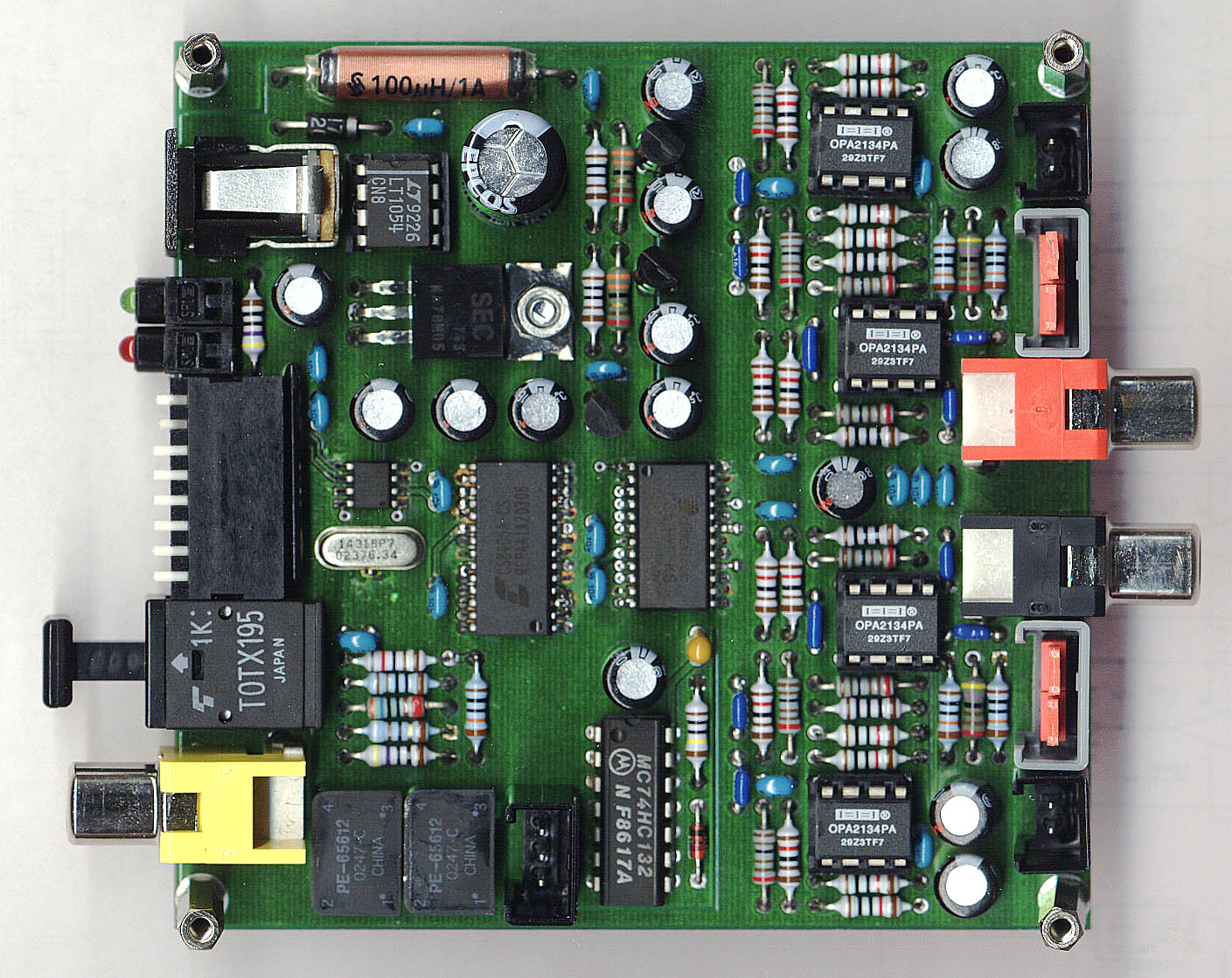
The latest circuit diagram of the AD2496 prototype (GIF) is shown here.
Power Supply
The nominal supply voltage is 12 V DC, but the device works from 8 V on. According to the specification up to 15 V are allowed. The prototype consumes 180 mA.
Analogue: The op-amps are supplied with +/-10 V approx. A LT1054 (100 mA / 15 V capability) generates the negative supply voltage. The voltage followers T1 and T2 furthermore stabilise the op-amps supply voltage.
Digital: A 5 V regulator is employed for the digital section and another low-power 5 V regulator generates the analogue supply and the reference voltage for the ADC.
Analogue Inputs and Input Amplifiers
The analogue input accepts both balanced and unbalanced signals. Balanced input signals (XLR-connector) can be connected through ST2 (ST5), where either the balanced or the unbalanced input (on-board RCA jack) may be selected with an additional external switch. If no balanced input is used, the indicated jumpers must be placed to select the unbalanced RCA inputs.
IC1 (IC3) buffers the input signal. The gain of this stage may be increased by additional resistors (or potentiometers) at ST3 (ST6). The subsequent 2nd order balancing low pass filter IC2 (IC4) not only rejects frequencies causing alias effects but also balances the input signals. It is therefore not necessary to rely on the balancing capabilities of the A/D converter CS5361.
The input sensitivity for full scale is 2.22 Vrms.
ADC
There is much to tell about the A/D converter CS5361, but here I just want you to refer to the the CS5361 data sheet. Let me say it this way: All necessary provisions are made so that the CS5361 operates
S/PDIF Transmitter
The CS8405A S/PDIF transmitter operates in hardware mode in order to avoid a microcontroller or other circuitry that makes it more difficult for others to reproduce the device. The transmitter converts the IIS data stream to an S/PDIF or AES3 signal and provides drivers to supply the outputs. The CS8405A is able to add lots of additional information to the data stream, but in hardware mode this is limited to some information that can be entered by the remaining pins. For experiments I provided switches to enter most of these information, though in practice they do not make much sense. See the "Set Up and Switches" chapter below.
Obviously there is an error in the CS8405A data sheet. The "Not Emphasis" input works inverse to the specification: If high, the emphasis status channel bit is set, and vice versa. As emphasis is rarely used, the emphasis input pin normally should be tied low. In the prototype I rewired it to the formerly unused switch 7.
Outputs
A coaxial and an optical (TOSLINK) S/PDIF output is provided. A three pin XLR connector for an AES3 interface may be connected externally through ST7. As requested by the standards, both electrical outputs are transformer coupled by transformers especially designed for digital audio interfaces.
Originally I planned to use the TOTX173 / TORX173 as the optical transmitter / receiver. These are commonly used TOSLINK devices. They work, but I found out later that they are specified only up to 48 kHz sample rate (6 MBit NRZ or 3 MBit bi-phase resp.) and so I had to go for something faster. My distributor recommended TOTX195 and TORX194 as they were available and pin-compatible to the 173s. They are for 5 MBit and industrial use specified which is sufficient. I found out that these devices are much more expensive compared to those for consumer equipment. Now I consider to use TOTX141P and TORX141P which are not pin compatible but for up to 7.5 MBit. However, though they are manufactured in high quantities and thus cheap they are really difficult to buy: Distributors offer industrial types only and consumer devices are directly sold to manufacturers of consumer electronics. See also Toshibas TOSLINK Fiberoptic Devices Overview.
Clock Generation
For all 4 sample rates the CS5361 and the CS8405A need 4 different clock frequencies MClk (Master Clock), which are generated by the MK1412A from ICS from a standard 14.3181 MHz crystal.
| Sample Rate | Clock Frequency (MClk) |
| 32 kHz | 8.192 MHz |
| 44.1 kHz | 11.2896 MHz |
| 48 kHz | 12.288 MHz |
| 96 kHz | 24.576 MHz |
Set Up and Switches
8 switches are provided for set up of the ADC / transmitter. Not all of them are used, and except for the sample rate set up the remaining ones are more or less useful for experiments only.
| Switch Nr. | Setting | Use | |||||||||||||||
| 1 | Sample rate low |
|
|||||||||||||||
| 2 | Sample rate high | ||||||||||||||||
| 3 | U (User) | Originally intended to be used as a serial data stream, this bit can be forced to a fixed position here | |||||||||||||||
| 4 | V (Valid) | Originally intended to mark each sample individually as valid, this bit can be forced to a fixed position here | |||||||||||||||
| 5 | Original / Professional |
|
|||||||||||||||
| 6 | No Copyright / Professional | ||||||||||||||||
| 7 | Emphasis |
For emphasis either the preamplifier or the ADC should provide
a 50/15 us emphasis, which at least the AD2496 does not. Emphasis is not available in the 96 kHz mode. |
|||||||||||||||
| 8 | Not used |
Note: 96 kHz is not standardized in the consumer format. The professional format should be selected at 96 kHz.
Critics and Possible Improvements on the Current Prototype
In contrast to the D/A-converter the A/D converter is pretty much "ready". In the prototype I changed some resistors to improve its noise performance and manually wired one more switch to enable the emphasis bit. The only thing left to be done ist to replace the TOTX173 or TOTX195 resp. by e.g. TOTX141P - not pin compatible unfortunately, and difficult to purchase. The MK4112A is discontinued and can be replaced by the MK2703 (not pin compitble).
Meanwhile I have some reasonable test equipment to measure and optimise the most important technical data. I tried 4 different op-amps: OPA2134, OPA2227, NE5532 and (not seriously, but I'm curious) TL072.
| Op-Amp | OPA2134 | OPA2227 | NE5532 | TL072 |
| Input Type | FET | Bipolar | Bipolar | FET |
| Input Noise Specification | 8 nV/sqr(Hz) | 3 nV/sqr(Hz) | 5 nV/sqr(Hz) | 18 nV/sqr(Hz) |
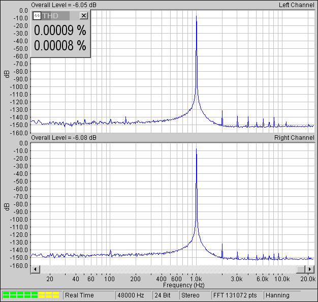
Total Harmonic Distortion
THD is very much depending on the op-amps beeing used. It took me a while until my measurements looked reliable enough to publish them. It's not just like connect, switch on, set-up and measure.The following values are measured by an FFT-analyser at 48 kHz sample rate and at an input level of -6 dB approximately. At this level distortion is least. Approaching full scale it rapidly grows up to 0.00060% (-104 dB approx.).
Measuring conditions for THD: Input frequency 1 kHz, level -6 dB, unbalanced input, all harmonics up to 24 kHz
| Op-Amp | OPA2134 | OPA2227 | NE5532 | TL072 |
| THD (left / right) % | 0.00009 / 0.00008 | 0.00009 / 0.00016 | 0.00011 / 0.00033 | 0.00030 / 0.00030 |
| THD (left / right) dB | -121 / -122 | -121 / -116 | -119 / -109 | -110 / -110 |
Note: The large difference in case of NE5532 betweeen left and right channel in all measurements always appeared again and I have no explanation for that. It remains even when the op-amps are swapped, but - very strange - with 96 kHz sample rate the difference is reversed to 0.00029% / 0.00017%. With the OPA2227 it is similar but not that extreme.
|
|
| Diagram: THD measured with OPA2134 |
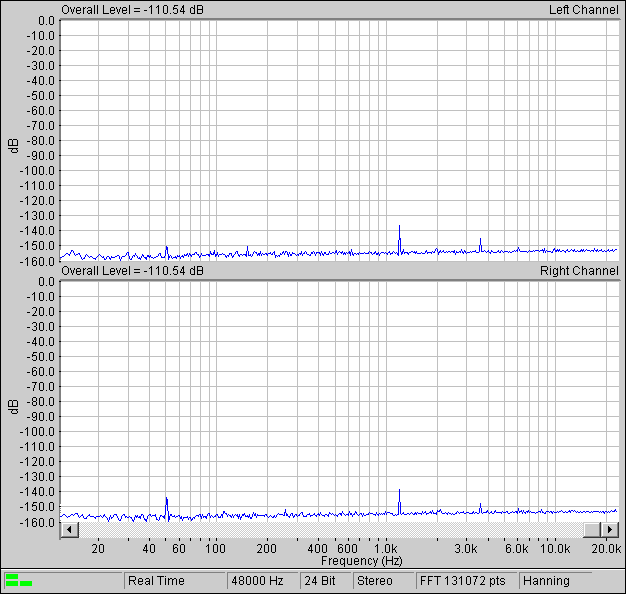
Noise Floor (Dynamic Range)
It turned out that relatively much noise was generated by R6 and R23. 10 kOhm is too much for an application like this. So these values were reduced to 1 kOhm.
Measuring conditions for noise: Inputs terminated to ground by 50 Ohm, unweighted (up to 24 kHz)
| Op-Amp | OPA2134 | OPA2227 | NE5532 | TL072 | None |
| Noise (left / right) dB | -109.3 / -109.0 | -110.5 / -110.5 | -110.2 / -110.2 | -107.0 / -107.0 | -111.4 / -111.4 |
Note: "None" means the bare CS5361 with inputs AC-grounded. The CS5361 is specified to have a dynamic range of 111 dB typically, unweighted, from 10 Hz to 20 kHz whereas the measuring bandwidth above is 24 kHz. As pure white noise only is involved, the bandwidth can be reduced to 20 kHz by adding another -0.8 dB to the level, so my CS5361 sample is 1.2 dB better than typically specified.
|
| Diagram: Noise measured with OPA2227 |
THD + Noise
Unfortunately my FFT analyser does not display the most interesting THD+N reliably, so there is no diagram as an example. But I managed to figure out the following results which can be compared to the specification of the CS5361 (and I swear, I didn't manipulate them to make both look that similar:-):
Measuring conditions for THD+N: Input frequency 1 kHz, level -1 dB and -20 dB, unbalanced input, bandwidth and all harmonics up to 20 kHz
| Op-Amp | OPA2134 | OPA2227 | NE5532 | TL072 |
| THD+N @ -1 dB | -103.6 dB | -104 dB | -103 dB | -103 dB |
| THD+N @ -20 dB | -89.8 dB | -91.3 dB | -91 dB | -87.7 dB |
Conclusion:
THD is best with OPA2134, but at other levels than -6 dB its benefit is not that relevant. Noise is best with OPA2227, but differences are little. The strange results with NE5532 probably should not be taken too seriously, so this device, as it is easily available and relatively cheap, is not a bad choice.
The test results are really fine, I'm very glad with them. It should be worth it to use the next better, much more expensive and pin-compatible CS3581, specified to have 6 dB better dynamic range and 5 dB better THD.
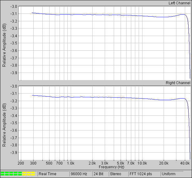
Frequency Response
Basically nothing special. The input filters are dimensioned so that they do not influence the frequency response given by the CS5361 noticeably. So the overall frequency response is what can be awaited:
|
| Figure: Frequency response |
Note: It is not that simple to measure the whole range in one sweep, so here it is shown from 300 Hz on only. At lower frequencies the response results from the input elements C1 and R4 (10 uF / 10 kOhm) forming a 1.6 Hz R/C high-pass filter and by the input high-pass filter of the CS5361 which is between 0.6 Hz and 2 Hz depending on the sampling rate..
Links to Some Related Data Sheets (updated April, 30thp, 2005)
| Manufacturer | Title | Device |
| A/D- and D/A-Converter | ||
| Linear Technology | Switched-Capacitor Voltage Converter with Regulator | LT1054 |
| TI / Burr Brown | High Performance Audio Operational Amplifiers | OPA2134 |
| TI / Burr Brown | High Precision, Low Noise Operational Amplifiers | OPA2227 |
| Texas Instruments | Dual Low-Noise Operational Amplifiers | NE5532 |
| A/D-Converter | ||
| ICS | MPEG Audio Clock Synthesizer (discontinued) | MK1412A |
| ICS | PLL Audio Clock Synthesizer (replacement for MK1412A) | MK2703 |
| Cirrus Logic | 114 dB, 192 kHz, Multi-Bit Audio A/D Converter | CS5361 |
| Cirrus Logic | 96 kHz, Digital Audio, Interface Transmitter | CS8405A |
| Toshiba | Fiber Optic Transmitting Module for Industrial Use | TOTX195 |
| Toshiba | Fiber Optic Transmitting Module for Digital Audio Interface | TOTX141P |
| D/A-Converter | ||
| Cirrus Logic | 24-Bit, 192 kHz D/A Converter for Digital Audio | CS4396 |
| Cirrus Logic | 96 kHz, Digital Audio Interface Receiver | CS8415A |
| Toshiba | Fiber Optic Receiving Module for Industrial Use | TORX194 |
| Toshiba | Fiber Optic Receiving Module for Digital Audio Interface | TORX141P |
| Last update: September, 27th, 2005 | Questions? Suggestions? Email Me! | Uwe Beis |