|
|
|
|
|
|
|
|
 General
Description
General
DescriptionThe word clock synchronization module XS-AD24, in conjunction with the AD24QS, features:
The power consumption of the ADC together with the XS-AD24 rises to 330 mA approx..
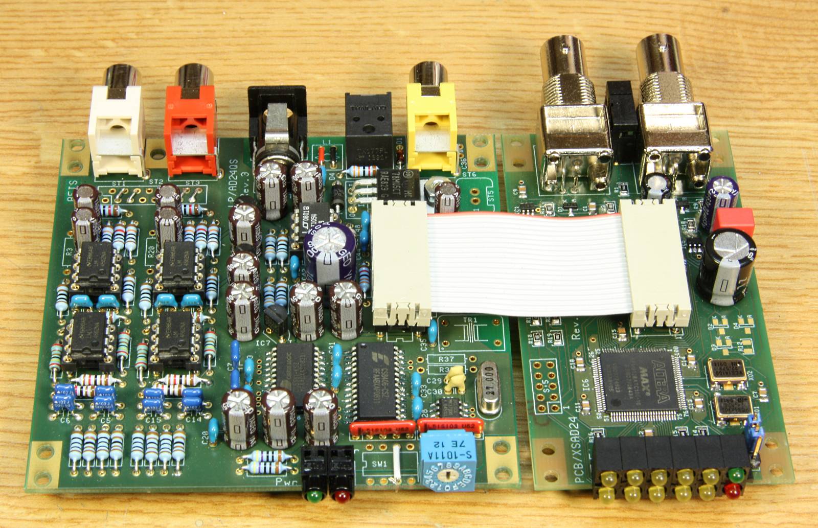
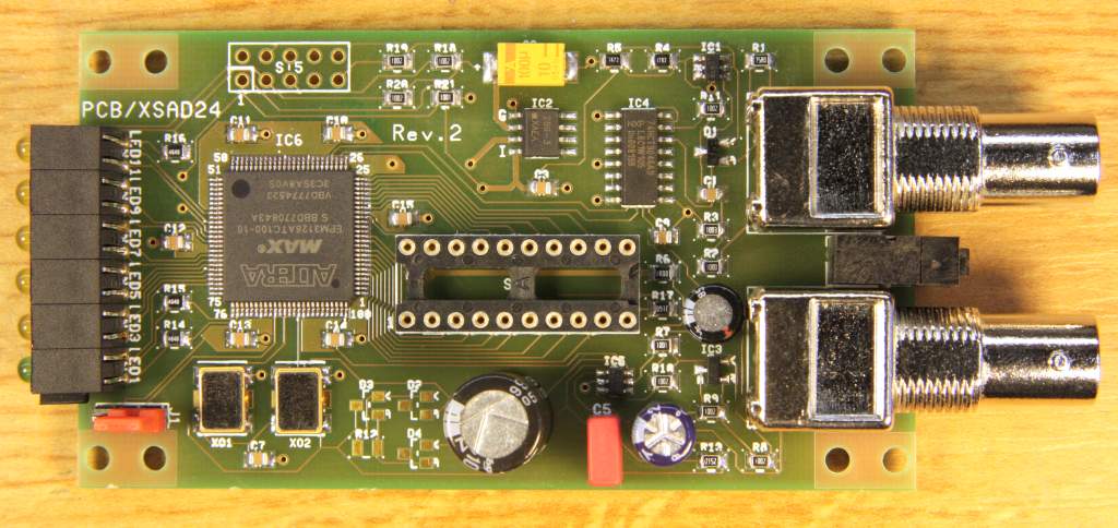
The XS-AD24 module is connected to the AD24QS by a 20 pin ribbon cable plugged into an IC socket that replaces the ADC's GAL. Also, the ADC's oscillator must not be populated or must be disconnected.
The size and shape of the PCB is designed so that it fits exactly
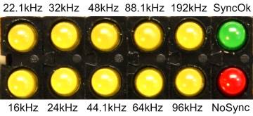
The frequency of any incoming word clock signal is compared by a CPLD whether it falls within one of the 10 bands that can be pulled-in by the VCXOs.
The algorithm that detects whether an incoming word clock signal falls within one of the 10 synchronizable bands is very fast. In the worst case (16 kHz sample rate) it needs 32 ms only and higher sample rates are detected proportionally faster.
In the first prototype I used self made VCXOs and that worked perfect. With the final VCXOs there is a slight problem which I did not yet solve yet: Particularly with the lower sample rates it takes a while until the PLL locks because after switching to "frequency ok" (green LED "Sync Ok" on) it does not lock fast enough, looses sync again, (LED off), restarts and it takes a short time until the PLL is finally locked.I still have to care for it.
 (Click
to enlarge)
(Click
to enlarge)
This photo shows the actual versin with PCB Rev. 2. Between the BNC-jacks is the 75 Ohm termination switch. With the jumper down left the word clock polarity can be changed.
Let me know you that there is a behavior in the XS-AD24 that is not as perfect as I usually expect from my designs, but I cannot simply correct it: Particularly when the default (free-running) frequency for the ADC is set low, the XS-AD24 tends to need a long time to synchronize to an incoming external sync signal. Set to a high or the same as the external frequency this behavior does not appear. E.g., when you set the the ADC's default frequency to 96 kHz, the XS-AD24 will always operate perfectly. (I would need one or two more terms in the CPLD to correct it, but I worked for days to optimize the CPLD and the next bigger CPLD is not only twice as expensive - moreover, it's available in BGA cases only.)
The XS-AD24 module is connected to the AD24QS by a 20 pin ribbon cable plugged into an IC socket that replaces the ADC's GAL, just like you can see in the photo at this article's beginning. On the AD24QS the ADC's oscillator IC MK2703 must not be populated or must be disconnected.
I propose you to proceed as follows: Build up the ADC completely as a stand-alone version including the oscillator IC MK2703. Before you solder it, bend the MClk output pin of the MK2703 (pin 5) slightly(!) so that e.g. a sheet of paper fits underneeth it. Than you can assemble and test the ADC completely. Afterwards, you isolate the prepared leg by pushing e.g. such a small pieces of paper underneeth the leg while you are re-soldering it. Also, I recommend to stop the MK2703's oscillator by tying its crystal input X1 (pin 1) to either ground or VCC (pin 2). Then you remove the GAL and plug the XS-AD24.
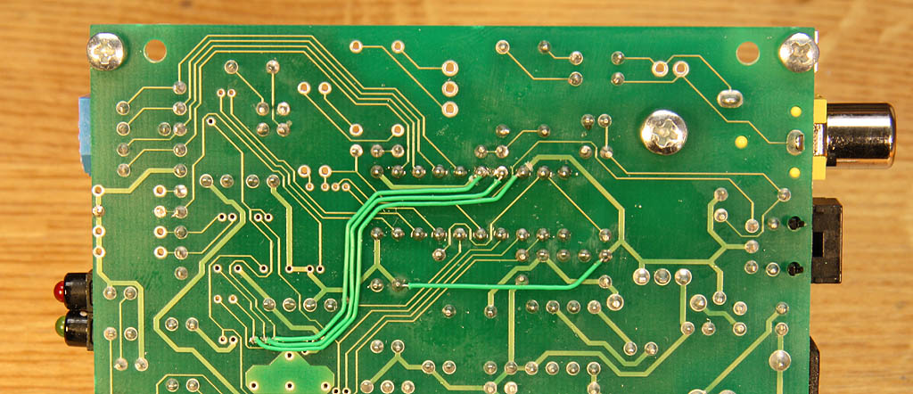 The
PCB for the AD24QS up to Rev.2 does not provide all signals that
are necessary to supply the XS-AD24 via the GAL's socket. Two
(or better three) signals, MClk, SClk and LRClk must be hand wired
to the unused pins 6, 7 and 8 of the GAL. These pins are currently
connected to VCC and must be disconnected. Should your GAL already
be socketed and you are happy that you don't need to unsolder
the GAL: Sorry, you must unsolder the socket even though because
one little track between its pins 7 and 8 on the component side
underneath the socket must also be cut :-(
The
PCB for the AD24QS up to Rev.2 does not provide all signals that
are necessary to supply the XS-AD24 via the GAL's socket. Two
(or better three) signals, MClk, SClk and LRClk must be hand wired
to the unused pins 6, 7 and 8 of the GAL. These pins are currently
connected to VCC and must be disconnected. Should your GAL already
be socketed and you are happy that you don't need to unsolder
the GAL: Sorry, you must unsolder the socket even though because
one little track between its pins 7 and 8 on the component side
underneath the socket must also be cut :-(
Also, the ADC's oscillator must be disabled as described above by isolating the MK2703's output pin 5. I sometimes unsolder and bend an already soldered IC leg upwards by threading some thin wire (0.1 - 0.15 mm) in a loop behind the leg and pulling both wire ends while soldering the leg. Though possibly not isolated, the leg is usually bent and lifted slightly than so that when it is heated again, a piece of paper can be pushed underneath it.
I made jitter measurements with the self made VCXOs. They resulted in the following table which shows the worst-case jitter performance of a word clock synchronized AD24QS system, i.e., both oscillators are running and the word clock generator's unknown jitter is included:
|
Jitter Frequency Hz |
Scale Reading dB |
Actual Jitter Value dBc/Sqrt(Hz) |
| 0.1 | -110 | -90 |
|
|
|
|
| 10 | -154 | -134 |
| 100 | not measurable | not measurable |
Click here to read the complete article about these jitter measurements. I don't intend to repeat these measurements with the new VCXOs because thay are labour-intensive and I don't expect mentionable or even significant differences.
Usually I design DIY-projects as far as possible in THT (through-hole technique). This one is almost a pure SMT (surface-mount technique) project because the CPLD, an Altera EPM3128, and other single-gate ICs are available as SMDs (surface-mount devices) only. The idea to make DIY easy by using THDs is so much spoiled by these SMDs that it would make little sense only to design the rest in THT.
Soldering the fine-pitch ICs is easy only when you a) have enough experience and b) when you have the appropriate equipment. Otherwise it may become a catastrophe. Also, I'd like to offer this module as a kit, too, but to compile kits with small SMDs (resistors etc.) is more or less a horror. Spare parts must be supplied: One of the resistors flipped out of my tweezer, I had no spare part and I searched for it for half an hour until I gave up.
This is why I decided not to offer the XS-AD24 as kits. Instead, I prepared a couple of completely assembled and tested modules. The CPLD is programmed, of course, and a 20 pin ribbon cable, 50 mm long, is included. Please understand that these modules are expensive (at least to my point of view), because purchasing all these (partially exotic) components for a handfull of modules is not only much work but also expensive. And don't forget that I assemble and solder them by hand and this is not just done with no bother.
I was often asked for word clock synchronization for the AD24QS but I had no solution. Not only that I had no hardware to offer - I didn't even have an idea how to fulfill my technical requirements for such an additional function. The voltage controlled R/C-oscillators (VCOs) that I used to see in commercial devices were not worth to be seriously considered as their jitter values are so high that any claims on the ADC's quality ought to be thrown overboard. Thus, the word clock synchronization should be based on voltage controlled crystal-oscillators (VCXOs) in order to maintain the ADC's original jitter quality when it is externally synchronized.
One problem is to find suitable VCXOs. They cannot be bought from stock, particularly not for reasonable prices(!). While 24.576 MHz is not an unusual frequency and a slight chance might exist to find one, I am convinced that there will be no chance for 22.5792 MHz. I did not (or could not) start this project until I found a good soul that promised to help me - I'm really grateful for that. And whoever will participate in this project should be so, too.
VCXOs can synchronize only to frequencies very close to their crystal's frequency, e.g., within +/-100 ppm (+/-0,0001%) or so, this is called the "pull-in range". I aimed that, when the external word clock frequency is outside of this narrow band, the ADC's oscillator runs on its native frequency, and when the frequency is inside of this band, the ADC's oscillator shall be locked to this frequency.
I also aimed that the ADC could easily be extended by the new module with just a simple connection. Once I had an idea how to do it (and the support for the VCXOs), I had to spend most of my time not with design itself, but to fit the necessary circuitry into an affordable CPLD. Only few readers may know how helpless you are when everything but one connection, one output or even one pin-assignment fits into the CPLD and the next bigger one is not only twice as complex but has also twice the physical size and is twice as expensive...
| Last update: January 7th, 2020 | Questions? Suggestions? Email Me! | Uwe Beis |