|
|
|
|
|
|
Introduction
The Design
Inside the FPGA
DIY - Do it Yourself - Hardware
DIY - VHDL (Software)
Related Links
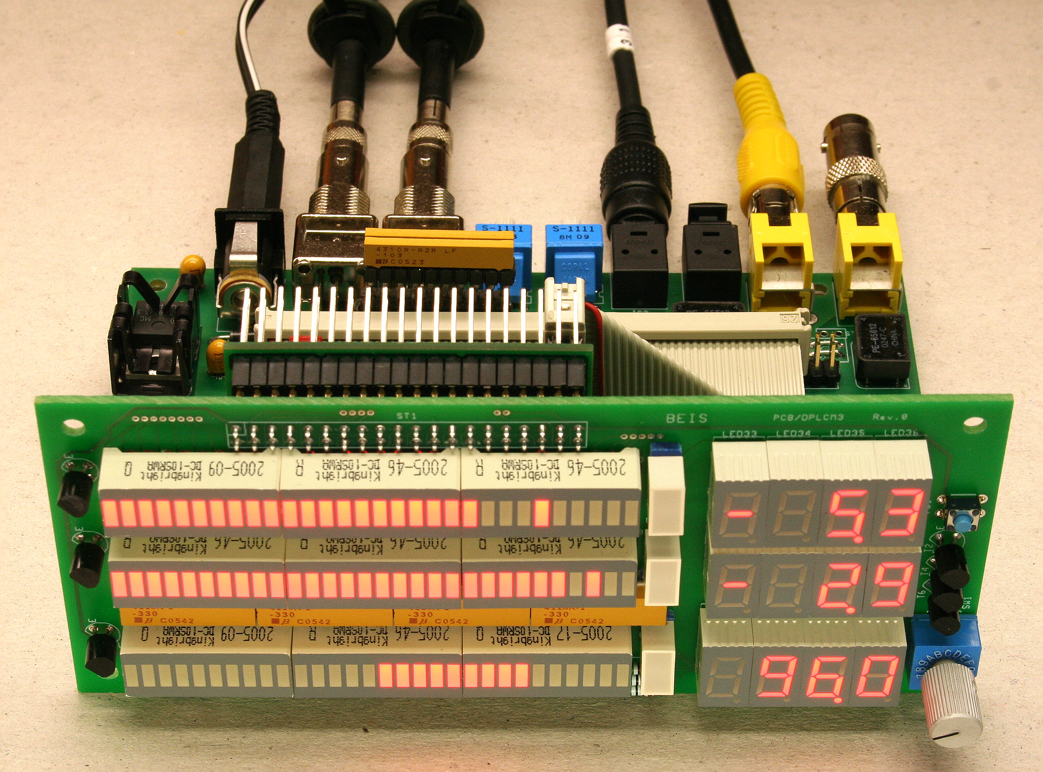
I started this project more to gather some experience with FPGAs, rather than to design or own such a device, but it ultimately developed into a complete design, consisting of several boards. It now looks like this:
The use of FPGA has several advantages over microcontrollers or DSPs for this application:
Of course, there is one disadvantage (no, it isn't the cost):
An FPGA design is not quite as common, and possibly more difficult
than a microcontroller design. Should you be interested in this
project, but intimidated by FPGA design and VHDL, it isn't so
difficult if merely wishing to modify a sample design such as
this.
Unlike VU and peak program meters, this peak level meter regards each audio sample individually, and thus can display the correct value of a single peak sample (i.e., its attack time is zero). Both VU and peak program meters incorporate a finite attack time, including an overshoot, in case of a tone burst. It's impossible for such meters to display exact digital levels, or clipping of the audio signal. The decay time of this peak level meter corresponds to that of a peak program meter.
Look how few components are necessary for this quite luxurious peak level and correlation meter:
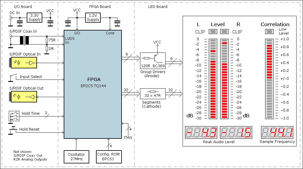
The DPLCM is divided into two (or three) parts:
Click here for the circuit diagrams of the FPGA development board 2C5-155 or the DPLCM-boards DPLCM-LED and DPLCM-I/O.
|
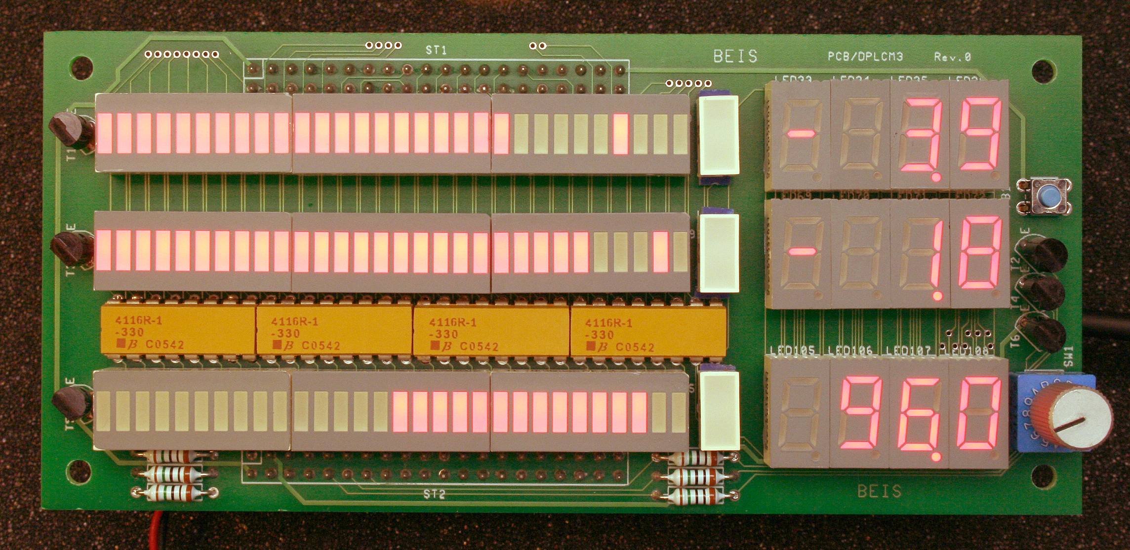
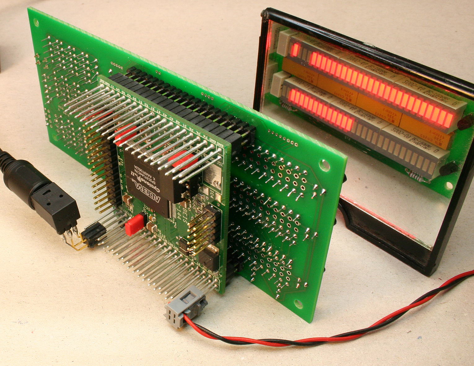
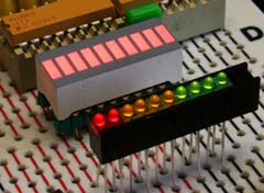
The LED board, with three 4-digit numeric displays (2 x peak level and sample rate), three 30-step bar displays (2 x level and correlation), and three additional indicator LEDs (2 x clip, 1 x low level for correlation) This board also contains the 32 limiting resistors for the LED cathodes, as well as 6 group resistors and transistors for the LED anode drivers. With the (optional) rotary or DIL switch, you can select the peak hold time. The pushbutton is for the peak hold release function. |
|
|
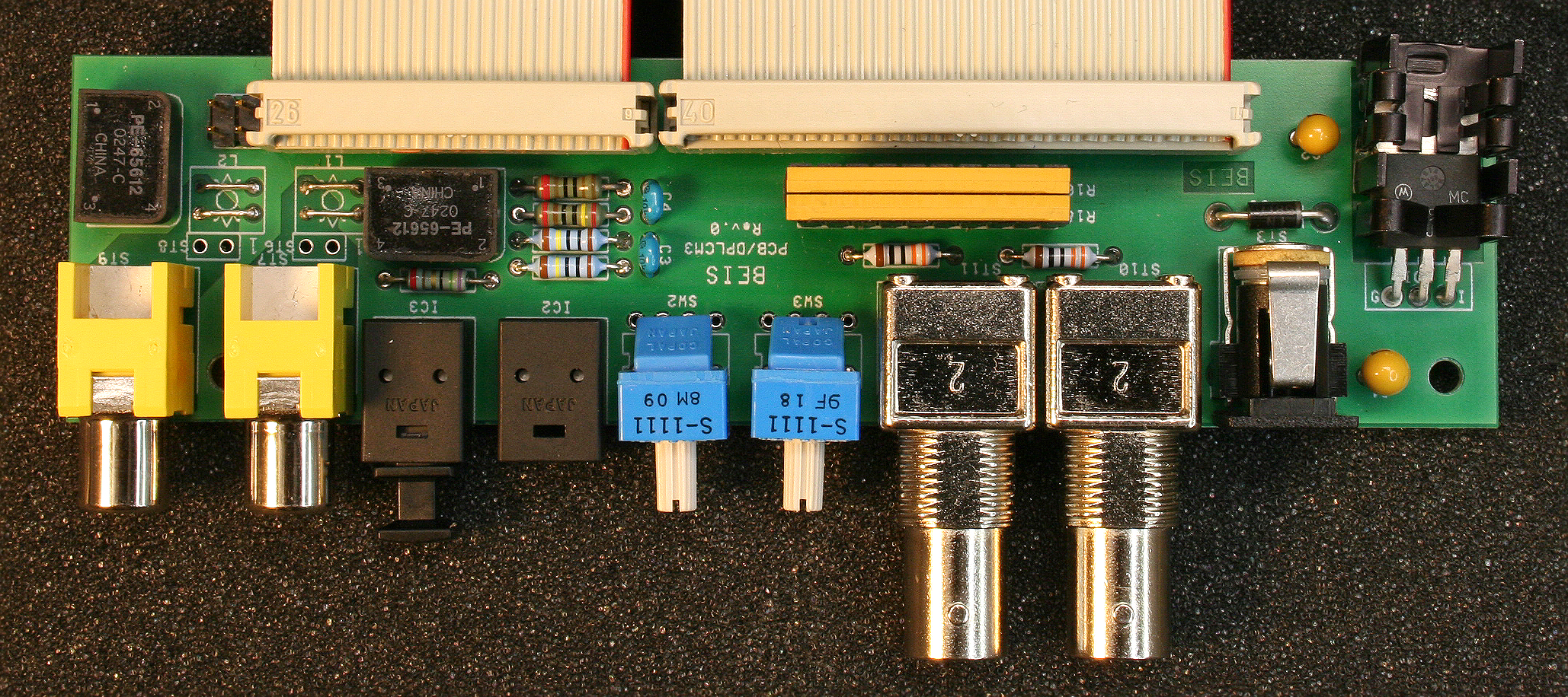
The I/O board is an option. Look at the next chapter "I/O Board Options" for details on it's functionality. | |
|
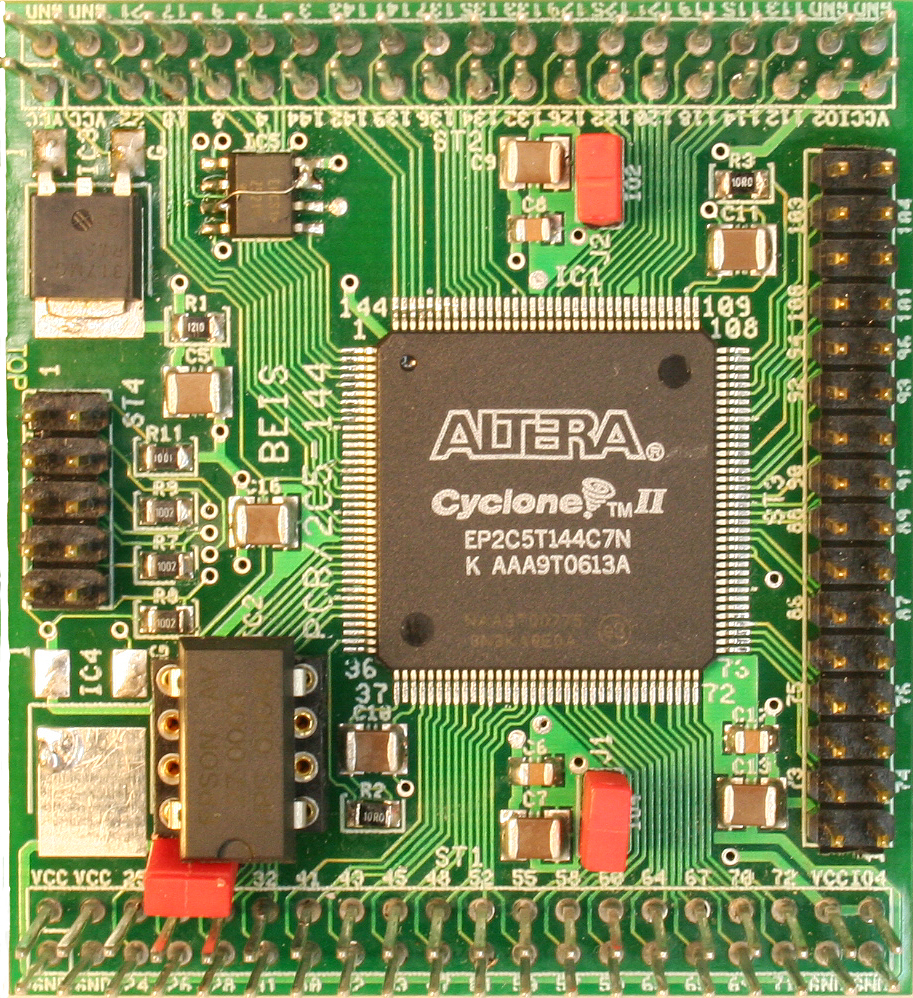
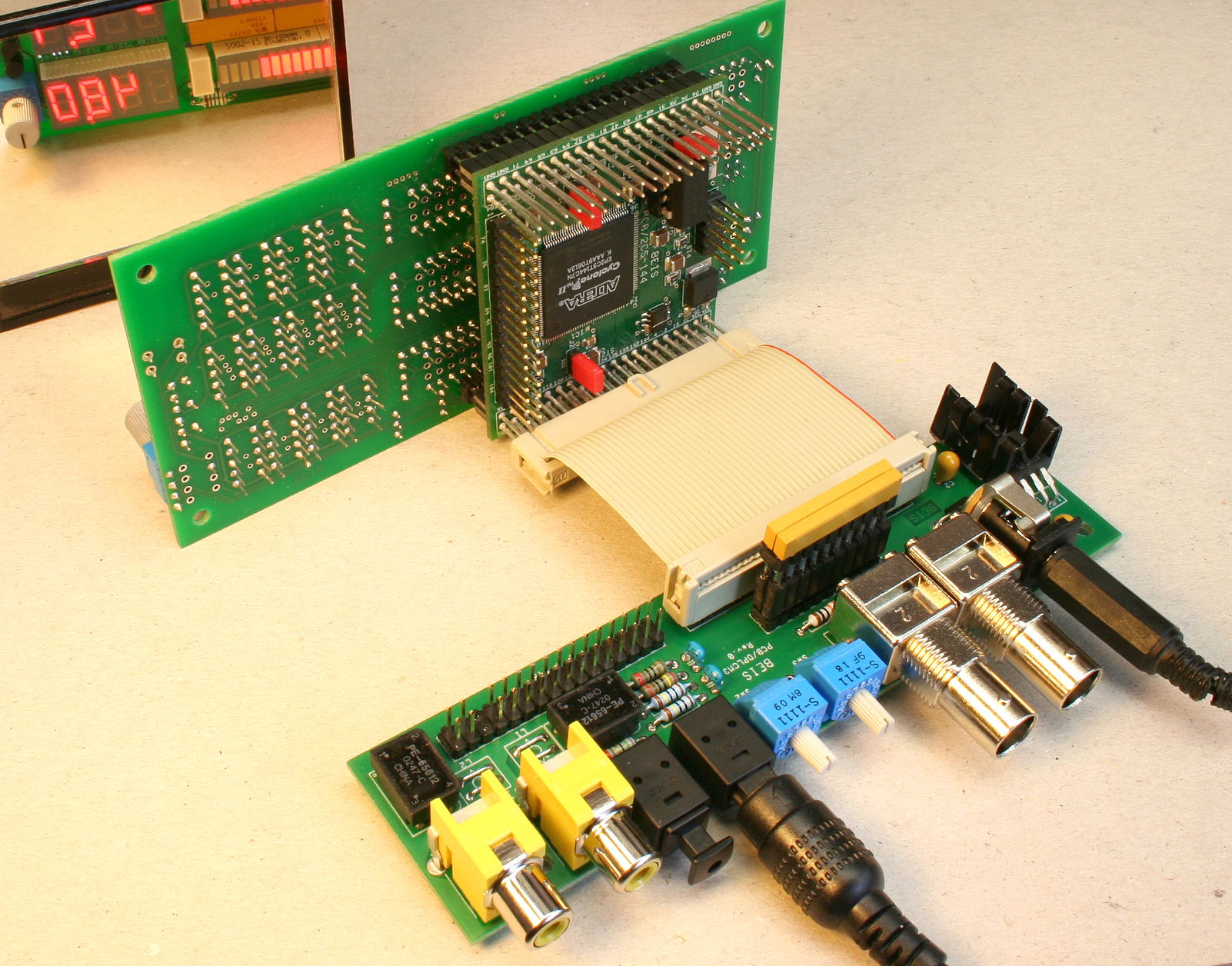
The FPGA development board contains little more than the minimum components necessary to run the FPGA. It is intended to be equipped with stackable 1/10" headers, so that it can be plugged directly behind the LED-board with it's bottom side, and connected to the I/O-board from it's top. For the DPLCM, this board need not be fully populated, e.g., the 2.5 V regulator can be omitted, and instead of the 32 pin stackable header, a simple 26 pin header could be used. |
|
Without the I/O board there is only one S/PDIF optical input available. The optical receiver must be connected externally by wires. | |

|
With the I/O board, it looks much more luxurious and provides:
On the I/O-board the switch "Hold Time", which also is provided on the LED board, is paralleled. |
|
|
Another option is to use a simplified I/O board connection to the FPGA board. In this case, the second ribbon cable can be omitted. Only these functions on the I/O board remain available:
The I/O-board also contains a "Hold Time" switch, which is a duplicate of that provided on the LED board. |
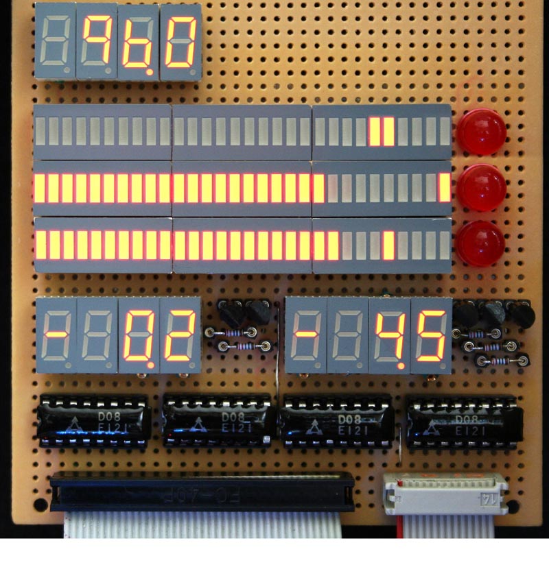
The LED board looks like this:
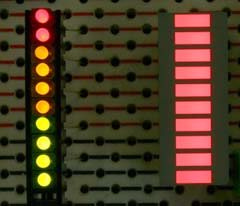
At the top left, you can see the left and the right channel level display. Each bar display consists of 30 LEDs, and displays the peak audio level. Originally I used steps of 1 dB, but now I turned to a non-linear dB-scale from -66 to 0 dB. The rectangular white objects to their right, are the clipping LEDs, and further to the right, are the left and right channel peak hold displays (showing -3.9 dB and -1.8 dB). The lower left bar, is the display for correlation (scaled from -1 to +1), accompanied by one more LED to indicate when the input levels are too low for correlation measurement. The sample rate display is at the bottom (showing 96.0 kHz).
For the high intensity LED bar displays I used DC10SRWA from Kingbright. They are fine, but for the 7-segment displays, I turned to VS Optoelectronic, as their LA3671-11EWAK displays seem to be significantly brighter than Kingbright's SA36-11SRWA. VS Optoelectronic's Bar-Graph Array LL-10000-SRWD should be as equivalent to the ones from Kingbright (and possibly a couple other manufacturers).
|
Another option for the LEDs, is to use single colored LEDs with 2.54 mm-spacing, like the 1.8 mm WU-1-19 series from VS Optoelectronic (or others), preferably in holders for LED rows, like the WU-1810 series. Their light emitting area is smaller, they cannot be viewed as good from the side, but colored LEDs look much better, of course. But you'd have to decide in advance where the yellow and the red thresholds shall be. I do not have a board stuffed with this style of LEDs. |
|
This is the top level design file for the digital audio level meter. It is primarily comprised of the following components:
An S/PDIF receiver: This receiver handles the S/PDIF data stream sample rate, from 30, up to 200 kHz (corresponding to up to 12.8 MBit S/PDIF data bit rate), and automatically adapts to it (similar to a PLL). The S/PDIF data stream should be sampled at a minimum of 80 MHz, but I suggest using 100 MHz or 108 MHz (= 4 x 27 MHz). The oscillator, by the way, needs to operate at only a fraction of that clock frequency (e.g. at 50 or 27 MHz).
The FPGA can be connected directly to the output of a TOSLINK receiver, but not the popular TORX173, as this one operates with 5 V only, and moreover, can only handle up to a 48 kHz sample rate. I used the TORX141P, for up to 96 kHz. I also provided the direct connection of a transformer coupled coax-input, using the LVDS capability of the FPGA. It worked fine, and should be usable up to 196 kHz or more, but the LVDS input specifications were not very well adhered to, and I can't guarantee that it's ok to do it this way.
After a rough estimation of the S/PDIF bit rate, the sample rate is detected more precisely (similar to a PLL). This S/PDIF signal sample rate, which of course depends on the audio sample rate, is twice as high as the S/PDIF data rate (i.e. up to 25.6 MHz). It is not, like with a PLL, exactly twice as high, but close to it only. The moments of input signal sampling are approximated as closely as possible to the ideal ones (i.e. those of a PLL, generated with a fixed phase and frequency relation to the input signal). As this approximation must be done using the constant, crystal-controlled clock rate of the FPGA, the sample rate cannot be reconstructed as jitter-free as an analog PLL can. Thus, due to the strong jitter, it would not make much sense to build an S/PDIF transmitter, operating synchronously to the received signal.
The S/PDIF receiver, outputs one or two 24-bit audio signals (single-channel / dual-data rate should be supported, but has not been tested). It also outputs the Validity, User Status, Channel Status, Parity bits, and a few clock, index and enable signals needed to run subsequent circuits. The S/PDIF receiver does not decode the Channel Status data stream, so there is no access to the copy protection signal and other information, which may be available there.
The peak level meter operates like an ideal full wave rectifier, with a capacitor, and a discharging resistor. Like the full wave rectifier, it builds the absolute value of the audio input signal. So, for the audio level, one bit less is needed than for the audio signal. The level value "charges the capacitor" instantaneously (the attack time is zero). Following the standards for a PPM (peak program meter, German DIN specification 45406), the "capacitor is discharged" 20 dB within 1.5 s (i.e., 650 ms decay time constant). The audio level signal is calculated and updated each millisecond.
For the LED bar display, the audio level determined by the peak level meter is converted to a logarithmic value, using a somewhat "brute force" counter method for the conversion. The converted value has a resolution of 0.1 dB, and as a 23-bit word size corresponds to a dynamic range of almost 140 dB, the binary decibel value spans 1375 steps.
The logarithmic converter also converts to a decimal logarithmic value, with a resolution of 0.1 dB, which is used for the peak level display.
The peak level is detected by this hold circuit and stored until either:
Under normal circumstances, each time a new peak audio level is detected, this new level is held for e.g. 1.5 s, and then falls back to the current level. Each time the current audio level reaches or exceeds the current peak level, this timer is restarted. The hold time can be set externally (by means of pin strapping, or by a switch), from 0.5 s up to 3.5 s, in steps of 0.5 s. (1.5 s appeared ideal to me). It may also be set to "Off" (i.e. there is no peak level display). If it is set to "Infinite", the fall-back must be initiated by a manual push button.
There are two peak level display methods provided for each channel: one consists of two 4-digit, 7-segment decimal displays, with a resolution of 0.1 dB, and a range of -137.5 dB, up to 0 dB, while the other method involves an additional LED remaining lit in each of the bar displays.
When the fall-back time is zero, the decimal display shows the actual signal level, measured by the peak level meter, which is updated once every ms. When no signal is present (= digital zero), "----" is displayed. When the audio signal reaches its negative or positive maximum value (0x7FFFFF or 0x800000 respectively), it is assumed to be clipped, and the decimal display shows "CLIP", along with the corresponding "Clip" indicator being lit at the bar display.
Note: As 16-bit signals (e.g. from a CD player) can only reach 0x7FFF for negative signals (but not 0x7FFFFF), the clipping display for them, works for positive signals only (0x8000 = 0x800000). I actually observed a clipping indication from one of my CDs, but this did not imply that the signal was actually clipped. I rather assume that it was just perfectly normalized.
The correlation of both audio input channels, reduced to 9 bit, is calculated. The output is a signal between 0x0 and 0xFF, indicating the correlation (more specifically: the correlation rate) of -1 to +1. The display time constant is 0.5 s. Theoretically, this measurement is independent of the signal levels, however, when one input level becomes lower than approximately -30 dB, the correlation can no longer be calculated with adequate precision, and the "Low Input Level" LED is lit. With further falling input levels, the displayed correlation value is gradually reduced to zero.
Lastly, the actual sample rate is displayed by using a five digit decimal counter, where the first stage counts 10 Hz, but is not displayed. Also, this first counter stage is initialized by 5 (i.e. the counter's value is rounded by 50 Hz, so the display remains stable for a deviation from the sample rate by +50/-40 Hz).
During the first two seconds after power up, an LED test is run and the version code (4 digits) is displayed in the sample rate display.
LED multiplexing is performed in the top level design file. There are five displays to be multiplexed: left bar display, right bar display, left decimal peak, right decimal peak, and sample rate. All LEDs of one display, together, are called an LED "group". An LED group consists of 32 LEDs (the LED segments), and their associated signals. These six groups are multiplexed with 1 ms per group (160 Hz). In order to allow bipolar transistors (as group drivers) to get out of saturation, the group drivers must be switched off 10 us before the segments for the next group are switched on. The current per-segment is 20 mA approx., so the group driver transistors need to switch up to around 640 mA of current.
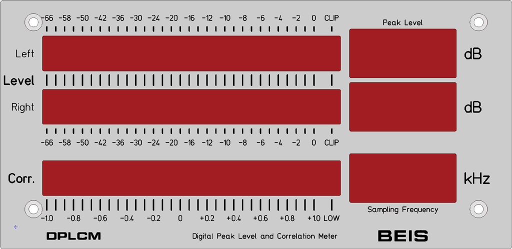
Unlike what is seen in the above graphic, the VHDL code contains a non-linear scale for the level-LED bars. The first 12 LEDs are stepped in 1 dB increments, and the remaining 18 LEDs are arranged in 3 groups, with 6 LEDs each and stepped 2, 3 and 4 dB resp., so that the LED with the lowest value is lit at -66 dB. Refer also to the draft below, for a front panel image of the scale.
Now that I have complete and tested board layouts, I would like to share it with other DIY'ers and prepare some complete kits. Some of the components I can't get in small quantities, others would be quite expensive. This means that preparing kits will be worthwhile only if there are enough interested participants. I have no idea if this will be the case, so I'll likely wait until I get enough requests for kits or boards. By "enough", I think I would need around 15 requests.
There are several possibilities for the construction of this project, each requiring different levels of DIY skills:
Then, there is always the option of buying the material partially or completely yourself. If this project shows a substantial amount of DIY community interest, and the quantity of parts I can purchase is high enough, I should be able to offer it as cheap as you would normally get it (hopefully a little cheaper), so I intend to offer:
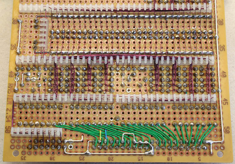
The latter option (the FPGA module only) is useful if you want to implement an LED layout different than mine. You can either design your own PCB, or put the LEDs on a prototype board using the VeroWire system, etc., as I did with my prototype. That doesn't usually take too long, and is technically and visually acceptable:
Should you want to join the project, send me an e-mail (please excuse the inconvenience to find out my e-mail address) and let me know which option you would prefer:
How to prepare the FPGA module:
Obviously, no one would want to wait for years until there were enough participants. So please let me know:
I'll keep you informed about the state of interest for this project.
I'm guessing the complete kits, with the FPGA module, complete and tested, would have the most appeal. I would expect prices such as:
You would need either the complete kit plus the FPGA module (estimated 185.- €), or the partial kit plus the FPGA module (estimated 130.- €)
This chapter will continue, should the DIY project begin.
I have not prepared an enclosure (yet?), but eventually, I will likely do so. You can find both board's dimensions here. As an enclosure, the SG215 shell case from the (German) company Fischer Elektronik should be fine (75 x 150 x 150 mm, a little too high and too deep), and for the front and rear panels, I would recommend using the service offered by Schaeffer AG (in Europe), which is also available in the US as Front Panel Express, LLC.
|
This is a draft for a front panel fitting for the SG215. Here you can find the design files for the aluminum front panel and the red transparent acrylic window panel fitting into the openings of the front panel. For other enclosures you can edit these design files using the Front Panel Designer from Front Panel Express, LLC (or, in Europe, the "Frontplattendesigner" from Schaeffer AG). But note: These front panels are not cheap. |
I'm not actually sure if VHDL code would be called "software", or if it belongs to the hardware. Nevertheless, for the sake of distinction, it's easier to simply refer to it as software.
Should you want to modify or work on the code, you'll need the Altera Design Software. It's available for free. Should you also want to download the modified software into the DPLCM's FPGA, you would need:
|
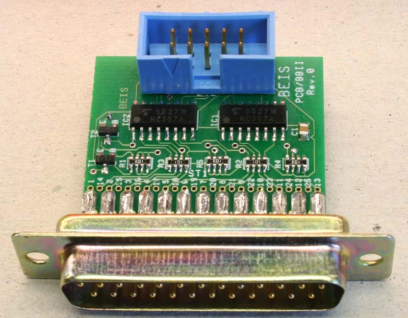
The cable shown here is actually a small PCB, but Altera sells this as a complete cable. You'll need this in order to program the FPGA, or the configuration IC. Altera offers several programming adapters. The "Byte Blaster II" for the parallel PC-port costs about 150 € (or Dollar), but you can easily build the Byte Blaster MV yourself. I found several circuit diagrams for it on the internet. Should the DPLCM become a DIY project, I may provide a kit for the download cable as well. The board is already designed and is functionally compatible to a Byte Blaster II, but for 3.3 V only. |
There isn't much to say about the code. I'm hoping it is sufficiently commented. Almost only STD_LOGIC and STD_LOGIC_VECTORS are used (except for integers in conditional statements).
Should you be a professional VHDL programmer reading my code, please keep in mind: I am not. As mentioned, I made this design in order to learn about it, and I'm sure that it could be programmed much more professionally. Anyway, this simple code might help others to understand it a bit more.
I started this project using Xilinx, switched over to Altera for certain reasons, returned to Xilinx once more, and finally turned back to Altera again. I'm going to stay with Altera (unless I find out that Lattice is even better). The original design was started with a Xilinx Spartan 3, and now it is targeted for an Altera Cyclone II. Both are the cheapest and smallest members of the most modern and economic series.
With the exception of the correlation display, I wrote the code using the fewest number of manufacturer macros possible:
One macro is a 32 x 18 unsigned multiplier, and the other, a PLL for the Master Clock (MClk). Converting the PLL to a Xilinx DLL should be easy (or alternatively, an oscillator with an equivalent output frequency could be used). The correlation display uses a couple more macros, which would also need to be converted to Xilinx macros.
Without the correlation display, I do not need to specify time groups to guarantee the correct operation, pipelining, or any other method used to speed up the design - as it is, it is just fast enough, but with the correlation circuitry, the timing constraints, at least for that part of the circuit, must be specified.
First you have to install the Web Edition of Altera's Quartus design software. It's free, and to make it run, you only need to get a web license for it (see the links below).
Now, you need to "Open" a "New Project" (the "New Project Wizard" helps):
Note: These design files may be "under construction", and the versions on the website might be out of date and may contain something different from what I've listed above, etc.. So, in case you are really interested, email me for the latest versions. (BTW, in any case I very much appreciate when you inform me when you are working with it.) In April '07 the design files have been unchanged for one year and I successfully compiled the most recent DPLCM-version (DPLCM_060401) with the most recent Quartus-version 7.0.
These are the latest VHDL design files: DPLCM.ZIP. Apart from the VHDL files, this archive also includes the assignment file DigitalLevelMeter.QSF and a conversion setup file DigitalLevelMeter.COF. All files must be copied into the working directory.
The Assignment File "DigitalLevelMeter.QSF" (Quartus Settings File) contains all assignments made in the Assignment Editor. The most important ones are the pin assignments, but other assignments like timing, pin type, and more, can (or must) be done there. Of course, I had to prepare this file for the design, and you should use it for your experiments as well.
Now you should be able to start the compilation (e.g. by Ctrl-L). You'll get a final report like this:
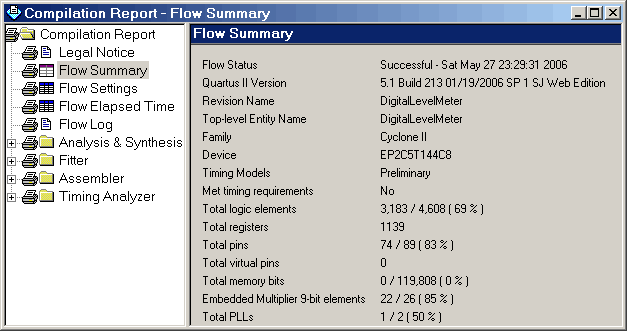
Don't be too concerned about the messages regarding timing requirements not being met. The next time you compile it, they will likely have been resolved.
Assuming your hardware is ready, all assignments were made correctly, and the download cable is connected to the JTAG-port, you now have to load the SOF file (SRAM Object File) into the FPGA:
The level meter should now run!
And now you can start to play with the VHDL code. Much luck and fun!
The FPGA configuration is SRAM-based (i.e. its configuration is lost when it is powered down). A non-volatile memory is needed to provide the FPGA with it's configuration data on power-up. For the final hardware, this so-called "serial configuration device" (usually an 8-pin serial FLASH-memory), must be programmed too. This can be done right through the FPGA, using the download cable, still connected to JTAG-port.
First you must create a JIC file, which can be downloaded into the target hardware. With the JIC (JTAG Indirect Configuration) file, first the FPGA is programmed to act as a "programmer" for the configuration device, so that the configuration data can later be programmed into it. To find out how to do this, look in the Quartus help menu for the corresponding chapter. This chapter is awfully difficult to find (I actually don't know where it is myself), so here is my way: "Search" for "Programming Devices with Flash Loaders" (including the quotation marks), and select the one and only search result. Click on "To program devices with the Serial Flash Loader:", and you'll find the few steps you'll need to perform. Or, you may look at the much more extensive documentation AN 370: Using the Serial FlashLoader With the Quartus II Software.
The necessary settings for this conversion are stored in the conversion setup file "DigitalLevelMeter.COF". I also added to DigitalLevelMeter.ZIP. Open this file in the "Convert programming Files" dialog.
Thanks very much to George Soffee, who read and corrected this text thorougly (I am not that good in English). He also pushed me to keep on working to make the display more DIY-compatible. (Actually, he is even still pushing me ;-)
| Last update: October 13th, 2015 | Questions? Suggestions? Email Me! | Uwe Beis |