|
|
|
|
|
|
When looking for an introduction to delta sigma conversion I found that most explanations were from a very theoretical point of view. It took me a while to understand how Delta Sigma converters really work. So I decided to write this introduction for people who prefer circuit diagrams to reading abstract equations.
To understand what I'm talking about you should at least be familiar with:
- Standard analogue techniques (op-amps, comparators etc.)
- Standard digital techniques (latches, binary codes etc.)
- Standard ADCs and DACs (resolution, speed)
- What a low pass filter is (at least an analogue one)
- The sampling theorem (sample frequency > 2 x input bandwidth,
alias effects)
Delta sigma converters are different from other converters. Note that I do not make a difference between analogue-to-digital (ADC) and digital-to-analogue converters (DAC). Both are very similar and what is realized in one of them using analogue signal processing circuitry is implemented in the other one using digital signal processing and vice versa. I will explain the delta sigma technique with the analogue-to-analogue delta sigma converter as the first object.
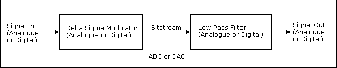
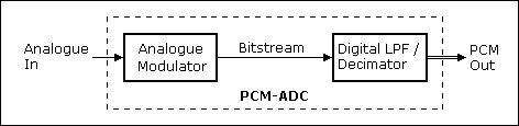
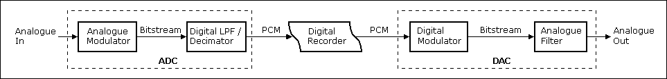
A delta sigma ADC or DAC always consists of a delta sigma modulator which produces the bitstream and a low pass filter.
The modulator will be implemented with digital technology if you have a digital signal source and in analogue technique in case of an analogue signal source. The same applies to the low pass filter: You will use an analogue low pass filter if you need an analogue signal output. A digital low pass filter will be implemented if you want a digital output. The digital low pass filter will probably be realized by a digital circuit or by an algorithm within a signal processor.
Before I proceed to the delta sigma modulator I would like to have a closer look to the bitstream and the low pass.
The bitstream can be regarded either as a digital or an analogue signal. The bitstream is a one-bit serial signal with a bit rate much higher than the data rate e.g. of the ADC. Its major property is that its average level represents the average input signal level. A digital "high" represents the highest and a "low" represents the lowest possible output value.
You can find a similar bitstream in a pulse width modulated (PWM) system but it has some disadvantages compared to the bitstream of a delta sigma modulator. The delta sigma kind of bitstream is also known as a pulse proportion modulated (PPM) signal. The serial transmission of numerically represented signal values (e.g. the serial output of a conventional ADC) is called pulse code modulation (PCM).
The low pass filter at the output is required, because you have to gain the average signal level out of the bitstream. You can regard the bitstream as a signal with its information in the lower frequency band and lots of noise above it. I presume low pass filters to be known and will not go into further deatils here.
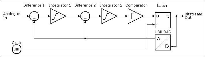
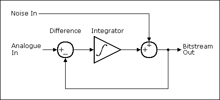
The delta sigma modulator is the core of delta sigma converters. As mentioned above it produces a bitstream. The average level of this bitstream represents the input signal level. A simple analogue first order delta sigma modulator block diagram looks like this:
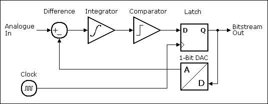
Please notice that due to the negative feedback loop the average(!) output level at the 1-Bit DAC must always be equal to the input signal level.
The digital counterpart looks just as simple:
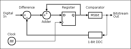
The comparator, just like in the analogue version, decides whether its input value is higher or lower than a certain threshold and puts out a single bit signal, the bitstrem. BTW, due to the preceding integrator this threshold is arbitrary. In order to obtain the bitstream in the digital modulator it is sufficient to strip off the comparator's input MSBit.
A 1-Bit DAC can output two different values only. They are termed VRef- and VRef+ and those of the 1-Bit DDC (digital-to-digital converter) DRef- and DRef+ correspondingly. In both types of modulators they determine its input range. Examples:
In the analogue modulator input ranges result out of the reference voltages as follows:
| VRef- | VRef+ | Input Range |
| 0 V | +1 V | 0 to +1 V |
| -10 V | +10 V | -10 V to +10 V |
Likewise, in the digital modulator the following input ranges are obtained:
| DRef- | DRef+ | Input Range | Type |
| 00 (hex) | FF (hex) | 00 (hex) to FF (hex) | Unsigned Binary Byte |
| 8000 (hex) | 7FFF (hex) | -32768 to +32767 (decimal) | Signed Binary 16 Bit |
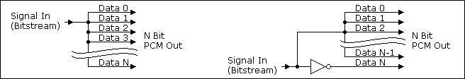
As a circuit diagram, the 1-Bit DDC may be as simple as a manifold of the input signal to all output data bits:
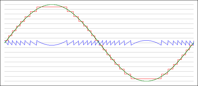
The first order modulator's signal diagrams look like this (Figure 2, analogue version):
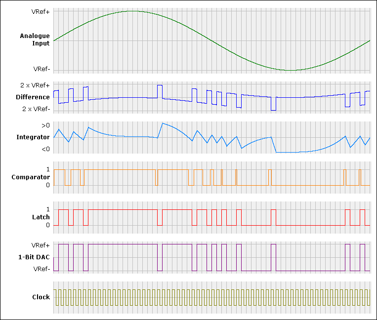
Note that in this example the clock rate, which here is also the sample rate, is 64 times higher than the frequency of the input signal. Conventional converters require a sample rate of more than twice the highest input frequency. Delta sigma converters require much more in order to produce a sufficient number of bitstream pulses. It is obvious: The more bitstream pulses are produced the better is the approximation of the input signal by the average bitstream.
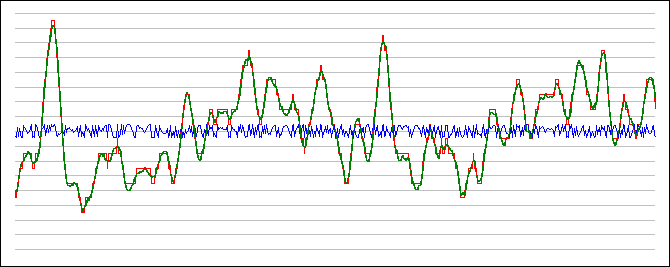
Once again: The average (low pass filtered) bitstream never(!) exactly represents the input signal. It is always(!) superimposed by some kind of noise.
One way to reduce this noise is to further increase the clock rate. Due to the sampling theorem the sampling rate must be higher than twice the maximum input frequency. Any further increase is called "oversampling rate". Example: Assume an audio signal with a bandwidth of up to 20 kHz (and probably slightly more). A typical sampling rate (for DAT etc.) is 48 kHz. In a typical delta sigma converter the clock frequency (which usually is also the sample rate) will be 64 x 48 kHz = 3072 kHz. This is equal to an oversampling rate of 64. In the example above (Figure 4) the clock frequency is 64 times higher than the frequency of the input signal. This means that the oversampling rate must be less than 32 for the given input frequency. (I don't know why only oversampling rates in the form of 2n are actually implemented. In my opinion any other form of this factor should be possible, too.)
Another - and better - way to reduce the noise is to use a higher order delta sigma modulator. Bitstreams produced by higher order modulators produce less noise at the low pass filter outputs. Normally this noise is random. First order modulators show some strong frequencies in the power spectrum (non-random noise or residual tones), which is disadvantgeous. If the input signal is close to the limits of the input range this effect is worst with first order modulators. If you want to know more about this refer to "First Order Delta Sigma Modulator Disadvantages".
A second order delta sigma modulator may look like this:
The bitstream of such a modulator is much closer to the ideal
pulse proportion signal than the one above so that
- either the input signal bandwidth may be higher,
- or the clock rate may be lower,
- or the output precision is increased (less noise)
whatever you want to achieve. Additionally "non-random noise"
is avoided to a great extent.
Delta sigma modulators of orders higher than 2 are possible to construct but they cannot simply be made by adding further stages as above. The reason is that the phase turn caused by more than two integrators will make the system unstable. Low pass filters are used instead. Delta sigma ADCs for audio applications typically use 5th order modulators and, as mentioned above, oversampling rates of 64. The architecture may look different, e.g. 2-bit DACs, but the basic principle of operation remains the same.
5th order and an oversampling rate of 64 - why that much?
As already mentioned within the average (low pass filtered) bitstream noise always remains. The amount of noise depends on a) the oversampling rate and b) the order of the modulator that produced the bitstream. Obviously it will not make sense to provide a 16 bit output to an ADC where the low 8 bit randomly change due to the remaining noise.
You may have heard that signals converted by ADCs suffer from quantization noise. Where does this come from? If a DC-voltage is applied to an ADC the output remains stable. It represents the input voltage more or less precisely, but without noise. So, where is there noise?
It's because the conversion is "more or less precisely"
only. A constant error in a DC measurement corresponds to a random
error or white noise (= noise with equal distribution over its
spectrum) in a conversion with a varying signal (AC). A digital
n bit signal can only settle to 2n values but the analogue
input signal may have any value. It is this difference between
the analogue value and its digital representation which causes
the problem. This is called the quantization noise. In the example
below a 4 bit ADC (= 24 = 16 quantization levels) is
assumed:
One can see that more quantization levels reduce the remaining
quantization noise. Using an ideal ADC with n bits the signal
to noise ratio (SNR) is:
n * 6.02 + 1.76 [dB] (or 2n * Sqr(3/2)) referred to
a full scale sine wave signal or
n * 6.02 + 10.79 [dB] (or 2n * Sqr(12)) referred to
the maximum peak-to-peak output voltage.
Thus for an ideal 16 bit ADC the SNR achievable is 98.1 dB and
the SNR for the 4-bit signal above is 25.8 dB.
Please note that conversion noise and not quantization noise is discussed here. Conversion noise appears already in the bitstream. Quantization noise appears only when signals are represented digitally. As mentioned above the amount of conversion noise depends on the oversampling rate and the order of the modulator. It can be expressed mathematically and results in the following graphs for delta sigma modulators with orders of 0, 1, 2, 3, 4 and 5:
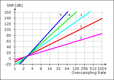
Now you can figure out which parameters (oversampling rate and order) of the modulator are required to obtain which noise. If a signal must be quantized, you may decide either the quantization noise or the conversion noise to be the bottle neck of the overall noise performance. In case that both shall have an equal effect, the overall SNR is reduced by 3 dB related to each of the noise portions.
Example: A 16 bit ADC, realized with a 3rd order modulator and a 64 fold oversampling rate would add -106 dB of conversion noise to the -98 dB quantization noise, so that quantization noise is prevailing and will be deteriorated by less than 1 dB only.
These SNR-figures are valid only for ideal converters. As so often in practice, the actually yielded SNR amongst others depends on the conversion speed and the IC-technology.
High quality ADCs for audio applications provide 24 output bits. They use 5th order modulators so that the conversion noise could be theoretically at -160 dB. The quantization noise of a 24 bit converter could become better than -147 dB. Real good ADC achieve "just" 120 dB SNR (19.6 effective bits) due to the non-ideal operation of the modulator (Example: Cirrus Logic CS5381). Nevertheless 120 dB is a fantastic value: 106 or 1:1,000,000 is close to the dynamic range of the human ear! Another 24 bit delta sigma ADC I know yields an SNR of 140 dB, but with an output rate of 7 Hz "only" (Linear Technology LTC2440).
The "conventional" way to explain Delta Sigma Converters is to look at the noise generated within the modulator and then to figure out how much noise remains after the low pass filter. This did not help me to understand what's going on inside the converters and so I disregarded this kind of view as yet. Let us have a short look on the mathematical background even though:
I want to describe the frequency response of a 1st order modulator like the one in Figure 2. But how to do it, when there are such strange, non-linear elements like comparators and latches in it? It took me a while to accept: The comparator/latch combination can be taken as an adder of noise to the output signal of the integrator, so a modulator block diagram like this results:
It can be regarded this way because a) the output of the modulator still contains the average input value and b) the (mainly randomly) "jumping" bitstream is a kind of noise - white noise to be more precise. Think about this or just believe me.
The frequency responses from both inputs to the bitstream output result from the integrator being
We can compute both frequency responses which for 1st and 2nd order modulators look like this:
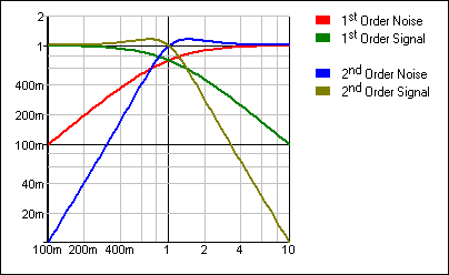
In the lower frequency band the desired input signals are passed and changed little, while the noise is suppressed to a great extent. With higher order modulators the noise is even more suppressed. This is called "noise shaping". And this is the reason why higher order modulators produce less output noise.
If you now start to compute noise figures depending on the modulators order and the oversampling rate you will get the SNR-diagram shown in Figure 8. For further details refer to the Intersil application note "A Brief Introduction to Sigma Delta Conversion". (Attention: Figure 6 "SNR vs Oversampling Ratio" is wrong. Use "my" Figure 8 instead.) I found another interesting introduction for various kinds of A/D converters including delta sigma:The Rane company: Digital Dharma of Audio A/D Converters.
I did not mention the term "decimation" yet at all because it is neither a process nor is it mystic - it's trivial. It is required when a bitstream, e.g. the output of an analogue modulator, shall be converted to a PCM signal.
The core statement is: Without losing any information in oversampled signals as many samples can be left out until the signal is not oversampled any more. (That's why it is called "oversampled"!)
Decimation takes place in delta sigma converters at the output of the digital low-pass filter. The bitstream is clocked with the sampling rate times the oversampling rate (e.g. 64 times the sample rate), and so the output of the digital low pass is clocked with the oversampling rate, too. But the sample rate clock (twice the input bandwidth) is required at the digital output only. Here decimation comes up: For an oversampling rate of e.g. 64 every 64th sample is taken, all others are discarded. This is possible because the signal is bandwidth limited by the digital low pass filter correspondingly. Quite simple - isn't it?
The feedback from the 1-Bit DAC to the block "Difference" introduces a lot of noise in an analogue modulator like in Figure 2. It is possible to reduce this noise by not only using one, but several bits instead. The comparator of Figure 2, which actually operates as a 1-bit ADC, is replaced by an N-bit ADC, and the latch and the DAC must be N bit wide, too:
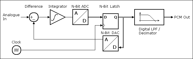
The modulator's output signal will also become N bit wide and thus can no longer be called "bitstream", but it is as suitable to be converted to a PCM signal as the single bit wide bitstream is. Because less noise is introduced, the oversampling rate may be reduced or the PCM output's width can be increased. This is why in practice multi-bit modulators are normally used in ADCs. Note: The modulator's internal signal width "N" is usually a few bits only.
Doing mathematical operations like adding two signals or multiplying a signal with a constant (or with another signal) or even other linear or nonlinear operations like filtering is easy to understand for PCM signals. But how to do this with bitstream signals? Any non-trivial mathematical operation on quantized signals significantly affects the lower significant data bits but a bitstream has no LSBits. The input is a one-bit signal and the output has to be a one-bit signal, too!
The first approach is obvious, but not very smart: Convert the bitstream to a PCM signal, do the desired operation(s) and convert the result back to a bitstream:
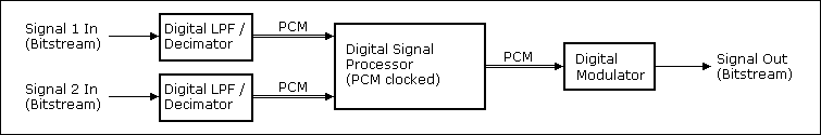
In practice, the digital signal processor in this block diagram may be a simple adder or multplier circuit. Also, there must not necessarily be a second bitstream input.
This "less smart" method takes one digital filter/decimator per input signal and one digital modulator for the output signal. Another issue of this method is the PCM clock (or sample rate resp.) which has to be introduced: A bitstream has no other sample rate than its bitstream clock, so that an arbitrary PCM sample rate ought to be chosen. This causes a loss of signal bandwidth due to the required digital filter and decimator.
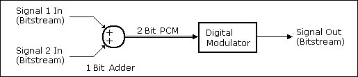
The second approach is a more clever way to do it: For example, what happens if you want to just add two bitstream signals (e.g., mix two audio signals) and simply add the bits of both bitstreams? You'll get a 2-bit signal (PCM, this not what you need), but its average level still represents the sum of the original input signals. We "only" need to convert this 2-bit PCM signal into a 1-bit one. Just one digital modulator is needed for that, not more, not less:
To understand this, we need a closer look on the digital modulator I explained in Figure 3. What I did not point out there is the fact that
Actually, the subtractor "Difference" in Figure 3 operates at the bitstream's clock rate and subtracts the 1-Bit DDC's PCM output signal from another, slowly clocked PCM signal. This subtractor is also able to subtract two PCM signals, both with the higher clock rate, of course. While the 2-bit sum of both bitstreams is not a usual PCM signal that represents the actual signal value at any time, it still can be viewed as a usable PCM signal for the digital modulator because it is sufficient when its temporal average value is correct. This, BTW, is very similar to the situation with the multi-bit signals in multi-bit converters.
Because the digital modulator's signal with needs only to be as wide as its digital input, in this example the circuit diagram for the digital modulator becomes quite simple as the bitstream adder's output signal is only 2 bit wide.
The general solution for mathematics with bitstreams looks like this:
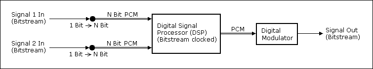
That's it. This "smart" solution takes no digital filter/decimator per input signal and only one (often quite simple) digital modulator for the output signal.
Alias effects: Delta sigma converters must run with sampling frequencies much higher than twice the maximum signal frequency (which is the minimum sample frequency of e.g. digital outputs). This has a very welcome consequence on alias effects: Only input signal frequencies close to the sampling frequency will be folded back and can cause alias signals as you can see in the graphic below:
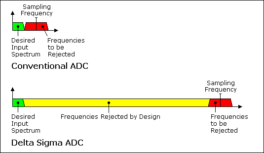
Thus it becomes obvious that conventional ADCs need expensive low pass filters in order to obtain a bandwidth close to the theoretical Nyquist limit. Delta sigma converters require simple RC low pass filters only and with a little more expense for a 2nd order filter one will get a virtually ideal behaviour. On the other hand an output low pass filter preceeding the decimator is required, which again can be realized more precisely, easily and cheap in digital techniques. Note that in practice the proportions are much more extreme than in the graphic above as due to limited space an oversampling rate of approx. 16 only is shown there.
DACs: The input signals of DACs are bandwidth limited by nature, so an input low pass filter is not necessary (it already had to be present when the digital signal was produced). An analog output filter is required anyway to suppress high frequency noise.
Infinite resolution of the bitstream: In analogue modulators the bitstream is sampled, but not quantized. It still has an infinite resolution just like the analogue signal has. It is superimposed by noise of course, but the more noise you filter out (the lower the low pass filter's frequency limit is), the more of the original resolution is usable - (theoretically) without limitation. This fact is also exploited by:
Direct Stream Digital (DSD) based devices: Traditionally digital devices use numerical representations of analogue samples, PCM in case of a serial signal. Delta sigma ADCs and DACs gain the PCM data out of the bitstream data (and vice versa) which is already a digital signal by means of low pass filters.
Why not record the bitstream directly? Conversion in delta sigma ADCs and DACs is executed in two steps each and as always each step has negative effects on the signal quality. Leaving out half of these steps - the filter in the ADC and the modulator in the DACs - should improve the performance of the complete system. Both, the quantization noise due to the limited number of recorded PCM bits and the conversion noise of the digital modulator would be dropped.

This is actually done on super audio CDs (SACDs). The whole system from the analogue input to the analogue output now requires only one modulator and one low pass filter instead of two of both required with conventional digital recording. Please remember: The bitstream of modern, high quality ADCs and DACs use an oversampling rate of 64, e.g. the amount of data is 64 bits for each audio sample - compared to 16 or up to 20 or 24 of conventional bits required for a comparable quality. Technically, SACDs are DVDs and based on a sampling frequency of 2.8224 MHz (= 2.8224 MBits net per channel). Not much that more than on audio CDs (0.7056 MBits net per channel), and no problem at all for a DVD with its high capcity.
Class-D Power Amplifiers:
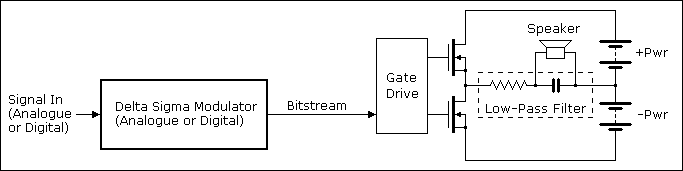
Both output transistors operate in push-pull mode, i. e., alternatingly one of both is conducting while the other one is switched off. Thus the bitstream is amplified to the high level of the power supply and is available at the output with low impedance. In order to regain the bitstream's mean value a simple LC-low-pass filter is sufficient in practice. A typical representative of this kind of amplifier is the LM4670, a simple and cheap low power amplifier with an analogue input, so simple that even the LC-low-pass filter is omitted and only the speaker's parasitic inductance remains as "low-pass filter". In contrast to that the TPA3200D1 is more complex, has higher output power and includes a digital (IIS-)input.
For the sake of completeness it shall be mentioned that for the operation of a class-D amplifier an analogue pulse width modulated (PWM) signal with a sufficiently high frequency can be used instead of the bitstream produced by a Delta Sigma converter. In contrast to digital pulse width modulated signals the pulse width ratios of analogue pulse width modulated signals are not quantized. With digital sources PWM operation does not suggest itself much, but with anlogue sources both techniques can be found in practice. In this case the pulse width modulator consists of a comparator comparing a triangle wave of e. g. a couple of MHz with the analogue input signal. An example is the TDA7490.
Compared to a conventional analogue class-AB amplifier, which advantages and disadvantages does such a class-D amplifier show?
In order to reduce both these disadvantages the supply voltage dependency as well as the output impedance can principally be lowered by degenerative feedback. But, if at all, this is by far not feasible in an amount as it is in analogue amplifieres as phase shifts inside the modulator and the low pass filter in conjunction with a degenerative feedback very soon lead to instabilities. Usually Delta Sigma amplifiers do not include degenerative feedback (as far as I experienced, at least). Once more, for the sake of completeness it shall be mentioned that PWM amplifiers do not incorporate phase shifting modulators so that degenerative feedback is much easier or much more efficient to achieve.
In analogue Delta Sigma based power amplifiers another trick is possible to drastically improve the signal quality:
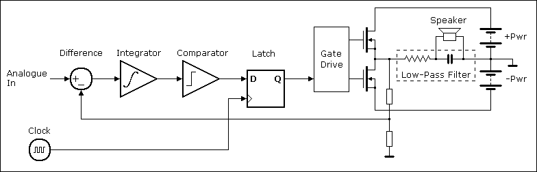
Compare to Figure 2: Instead of feeding back the bitstream via a 1-bit DAC to build the difference in this case a portion of the power transistor's output is directly fed back. Thus it is guaranteed that independent of all parasitic effects like supply voltage variations or the transistor's resistances the mean value at the low-pass input is always exactly proportional to the analogue input signal. Excellent performance is feasible by this concept. An example for that is the AD1996. Unfortunately, this trick works for amplifiers with analogue inputs only.
Conclusion: Class-D power amplifiers offer a much higher efficiency and less exhaust heat at the expense of their signal quality. Thus they are favourable for generic public address systems, where high power, small size and probably portability too, are required. They are less predestinated for high-quality audio amplifiers. Constructively the most critical elements are the output transistors: The faster they switch, the less the losses are or the higher the switching frequency may be. The latter, on the other hand, allows low pass filters with higher frequencies, which due to their less phase shifts within the signal band allow stronger degenerative feedback, so that the signal quality can be improved. With the advancing semiconductor technology class-D amplifiers will be increasingly utilizable for high-quality audio amplifiers.
Delta Sigma Converters or Sigma Delta Converters? Mankind does not seem to agree on one notation. Both notations are used equally often when you search via Google. I decided to stay with that guy who told he is living in the Mississippi Delta, so deltas mean something to him - and for him only the Sigma River may have a Sigma Delta... good point. Later I found out that the original name "Delta Sigma" was coined by the inventors Inose and Yasuda and "Sigma Delta" is actually not correct. I was lucky...
| Last update: November 26th, 2024 | Questions? Suggestions? Email Me! | Uwe Beis |