| |
|
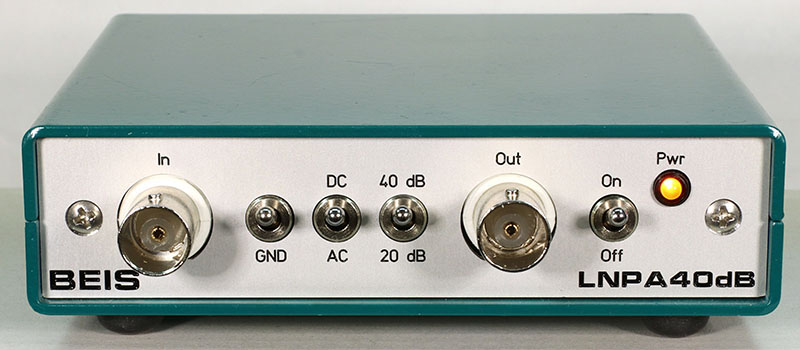
Low Noise FET Preamplifier
(![]() German Version: Rauscharmer FET Vorverstärker)
German Version: Rauscharmer FET Vorverstärker)
Battery powered, suitable for DC, audio and measurement purposes
Input voltage noise approx. 2.2 nV/√Hz
| |
|
Low Noise FET Preamplifier
(![]() German Version: Rauscharmer FET Vorverstärker)
German Version: Rauscharmer FET Vorverstärker)
Battery powered, suitable for DC, audio and measurement purposes
Input voltage noise approx. 2.2 nV/√Hz
The total input noise of (pre-)amplifiers consists of several components:
The preamplifier must amplify sufficiently so that no significant additional noise is added to the pre-amplified signal within the following signal processing chain due to input noise of the following stages or other causes.
The LNPA40dB (Low-Noise Preamplifier with 40 dB Gain) is optimized for audio applications, but can also amplify DC signals. It has FET inputs to avoid noise caused by input current noise at higher source impedances. It is battery powered because very low voltages with high spectral resolution are to be measured, and experience has shown that this is not possible with mains power supplies, because a connection to such a power supply would lead to enormous interference signals in the spectrum even with the best galvanic isolation in the power supply.
In this context, I would like to refer to other relevant links on my website:
The disadvantage of FET inputs, especially when using operational amplifiers, is that the best ones with about 4 nV/√Hz show an input voltage noise 4 - 5 times as high as the best bipolar operational amplifiers with about 0.9 nV/√Hz. On the other hand, the noise caused by the current noise of the input stage together with the source impedance exceeds that of the FET operational amplifiers even at relatively low source impedances. So:
For comparison: 0.9 nV/√Hz corresponds to the thermal noise of a 50 Ω resistor, 4.5 nV/√Hz corresponds approximately to the thermal noise of a 1200 Ω resistor.
However, it should be remembered that with all operational amplifiers at lower frequencies both the input voltage noise and the input current noise increase with decreasing frequency. The noise density of this so-called 1/√f noise is inversely proportional to the frequency, so it drops by 10 dB/octave. This is also known as pink noise. At higher frequencies the noise density is independent of the frequency, it is white noise. With bipolar operational amplifiers, the transition from pink to white noise occurs at much lower frequencies than with FET operational amplifiers. Many words, two pictures tell more:
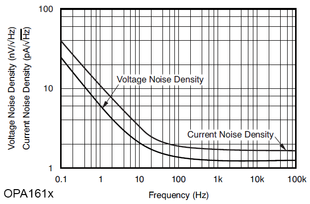
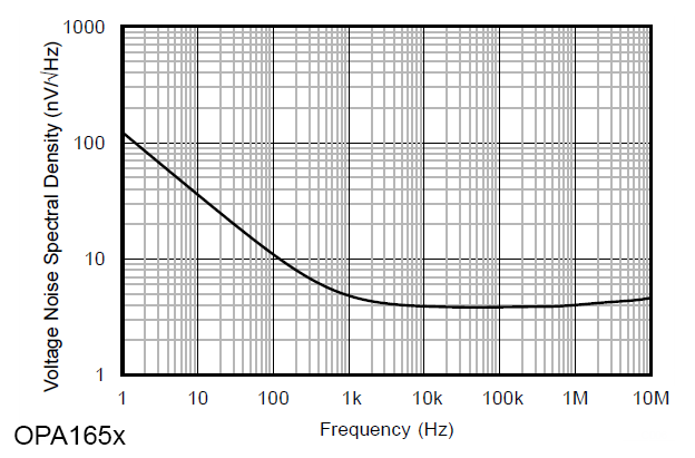
Voltage noise spectra of the operational amplifier series OPA161x and OPA165x
While the bipolar operational amplifiers of the OPA161x series have a pink to white noise transition of only about 20 Hz, the FET operational amplifiers of the OPA165x series have a pink to white noise transition of about 400 Hz. This is unusually high, but on the other hand it is lower with other FET operational amplifiers only because the white noise is higher, but not because the pink noise is lower.
You can also see that with the OPA161x at a source resistance of about 700 Ω the input current noise exceeds the very low input voltage noise and already at about 2.5 kΩ even the input voltage noise of the OPA165x, at least at the higher frequencies.
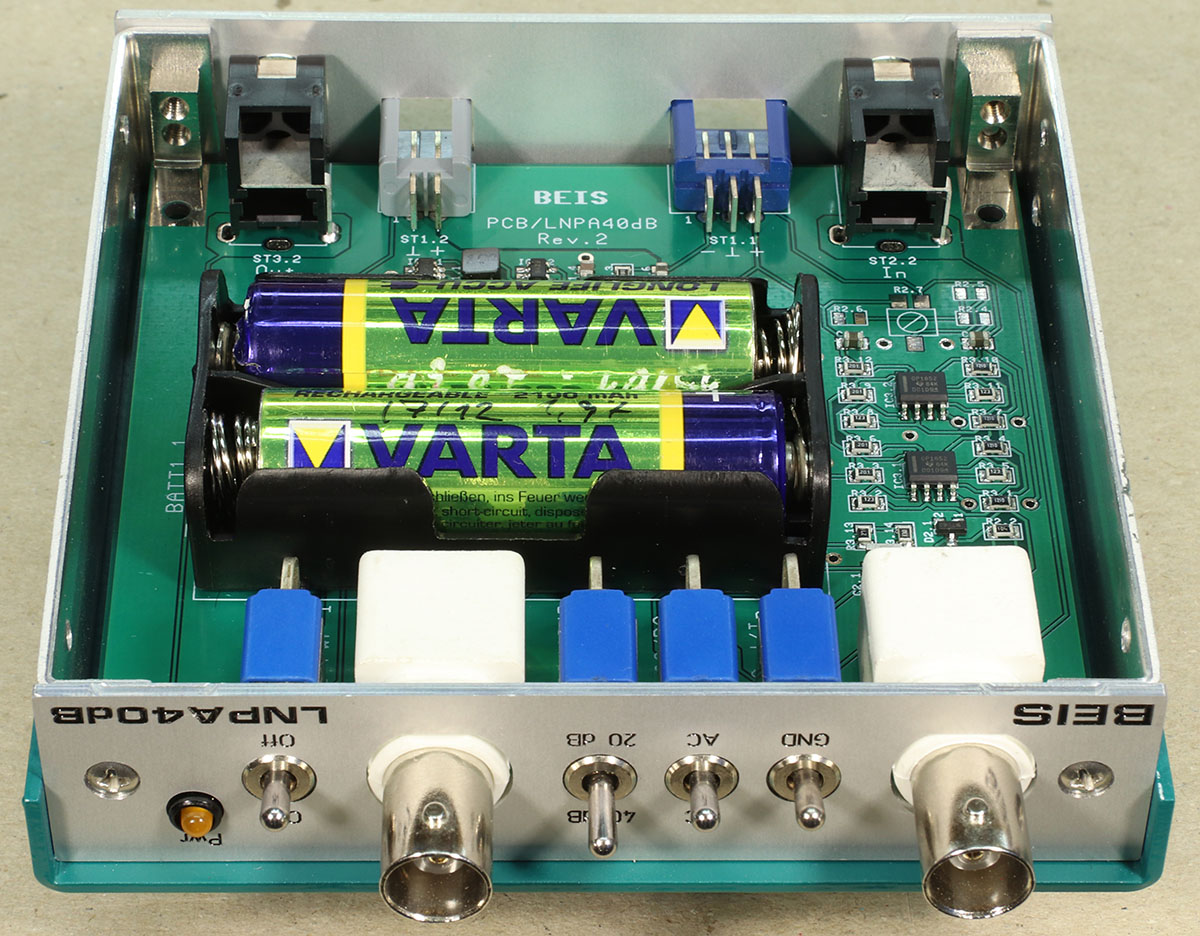 Because I found it an interesting method to reduce the input voltage noise of an amplifier by connecting several input stages in parallel, and because this is of course also desirable, I decided to use 4 FET operational amplifiers with lowest input voltage noise as feasible connected in parallel. I chose the dual version OPA1652, the OPA1612 can also be used in one assembly variant, but I don't know if I will ever try or use it.
Further characteristics and technical data are:
The LNPA40dB is installed in a 100 x 100 x 25 mm³ shell housing SG 206 from Fischer Elektronik. The component side points downwards, so that the batteries can be changed via a cover in the bottom of the housing.
Noise measurements:
To display the noise spectrum of the LNPA40dB, the output signal of the preamplifier was routed via a 192 kHz/24 bit ADC with a sensitivity of -1 dBV (= 0.89 Veff) for 100% FS and via USB to the PC, where the spectrum was calculated with ARTA. Each spectrum was calculated with 65536 samples, resulting in a resolution of approximately 2.9 Hz. In order to obtain smooth and precise curves, approx. 5000 to 10000 spectra were averaged per measurement, resulting in a measurement time of approx. 30 minutes per measurement. In addition there was a multiple of the time I needed to get the whole setup so clean and error-free that the measurements became as perfect as they look now.
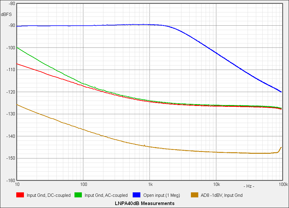
Different noise spectra of the LNPA40dB
Red: The input of the LNPA40dB is internally connected directly to ground (switch GND).
Green: The input of the LNPA40dB is switched to AC and externally connected to ground.
Blue: The input of the LNPA40dB is open, only its internal 1 MΩ input resistor is at the input.
Yellow: For comparison the inherent noise of the ADC, which is far below the output noise of the LNPA40dB.
With the input directly to ground (red) the input noise is lowest. With AC coupling (green), the internal 1 MΩ input resistor generates a noise current via the 100 nF coupling capacitor and thus a noise voltage that is higher than the input noise of the amplifier at low frequencies. If the input is open (blue), the full noise of the internal 1 MΩ input resistor can be seen. The input capacitance of the amplifier of approx. 80 pF together with the input resistance results in a low-pass filter with a cut-off frequency of approx. 2 kHz.
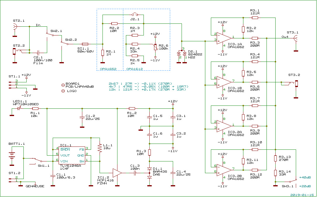
The internal operating voltage of approx. +12 V is generated from a step-up converter. The TLV61046A has an internal rectifier diode and starts at approx. 1.8 V. -11 V are generated from the +12 V with a FET driver IC controlled by the switching signal of the step-up converter. A particularly efficient LED displays not only the battery voltage, but also the internal +12 V voltage in an energy-saving manner with only 1 mA.
The input signal is led through a small, very fast PTC fuse to protect against overvoltages. Overvoltages up to approx. 60 V are kept away from the operational amplifiers by a bipolar dual diode, which is specified for short peak currents up to 8 A per diode at discharge voltages of 6 - 8 V. I have not (yet) tested this - the damage would be too great.
For the optionally provided bipolar operational amplifiers OPA1612, an adjustable resistor network is used to compensate their input current.
4 operational amplifiers amplify 20 or 40 dB, their outputs, which do not deliver exactly the same DC and AC voltages, are output via 4 200 Ω mixing resistors as a 50 Ω signal.
As simple and obvious as the circuit looks, I made some mistakes and had to correct them before it worked. There have been 4 circuit and 3 PCB versions so far:
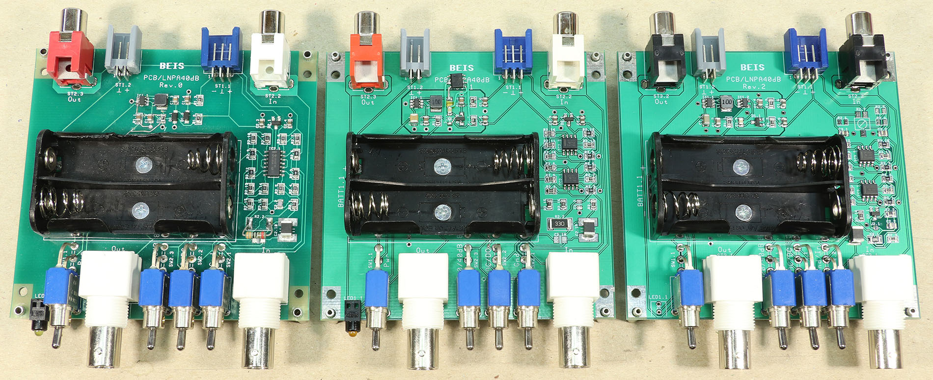
The (previous) 3 generations of printed circuit boards
In the first version I had used a 4-fold operational amplifier OPA1654. In the resulting layout, the input and output lines were so capacitively coupled that the amplifier oscillated with an open input at +40 dB. I could have anticipated that before. Also the 1 MHz oscillator frequency of the voltage converter was clearly visible in the output signal, although I would not have expected this due to the spatial separation of the circuit parts and multiple filtering of the operating voltages.
In the 2nd version I improved the input circuit and solved the problem of internal feedback with 2 x OPA1652, where the input and output lines can easily be separated spatially in the layout. Unfortunately, it turned out that the simpler circuit of the 1st version for generating the -11 V did not work in this setup, although I had adopted it unchanged. I was lucky - that a circuit only works by chance is not allowed to happen. With the newly introduced FET driver IC it worked securely.
In the 3rd version I introduced a much improved input protection besides the FET driver IC, the previous one would hardly have been suitable for more than ESD protection. A device for laboratory use should be more robust. Only a few "thinking errors" in the "greatly improved" input protection turned out after manufacture - if I had thought longer, I could have noticed it beforehand - so that it had to be revised again.
The 4th version is the above circuit, i.e. the latest version. PCBs of this version are available.
| Last update: April 7th, 2021 | Questions? Suggestions? Mail Me! | Uwe Beis |